
Introduction
The datapath is the part of the processor that holds and moves data: the registers, the ALU, the internal buses and the connections to memory. The control unit issues the control signals that tell the datapath, step by step, which register drives a bus, which register loads, what the ALU does and when memory is read or written. Each step is a set of register transfers (micro-operations) performed in one clock cycle.
GATE asks you to write or check the control sequence of an instruction on a single-bus or multiple-bus datapath, to count the clock cycles it takes, to compare single-cycle and multi-cycle implementations, and to apply the processor performance equation. How the control signals themselves are generated is the subject of Hardwired Control Unit and Microprogrammed Control Unit.
Prerequisites
- ALU Design and Multiplication: the ALU computes from two operands under a function select.
- Machine Instructions and Instruction Formats: the opcode and operand fields that the datapath decodes.
Core concepts
Registers of the datapath
| Register | Role |
|---|---|
| PC (program counter) | Address of the next instruction |
| IR (instruction register) | The instruction being executed |
| MAR (memory address register) | Address sent to memory |
| MDR (memory data register) | Word read from or to be written to memory |
| R0 to | General-purpose registers |
| Y, Z (temporaries, single-bus design) | Y holds one ALU operand; Z holds the ALU result |
Register transfer notation and control signals
means the contents of R2 are copied into R1. On a bus-based datapath each register has a gating signal that places its contents on the bus and that loads it from the bus. A transfer from R2 to R1 over the bus is the pair of signals in one cycle.
Memory reads are plus Read; the processor then waits for the memory to finish, signalled by MFC (memory function completed), with the control step WMFC (wait for MFC).
The instruction cycle
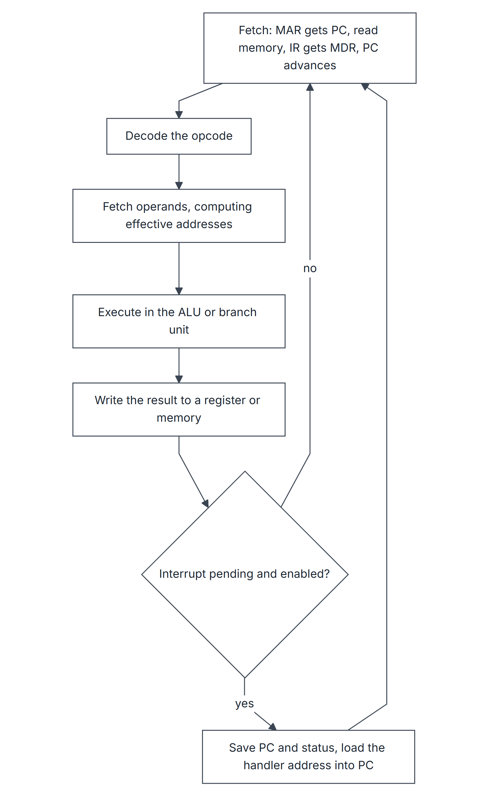
The interrupt check happens only between instructions, which is why an interrupt never splits an ordinary instruction; details are in I/O Interface and Interrupts.
Single-bus organisation
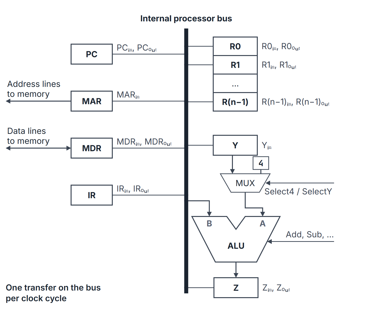
All registers, the ALU input and the MDR share one internal bus, so only one value can be transferred per cycle. The ALU's second input comes from register Y through a multiplexer that can instead select the constant 4 (to advance the PC by one 4-byte word); the ALU output is captured in Z.
Multiple-bus organisation
With three buses (two source buses A and B feeding the ALU, one destination bus C), a register file with two read ports and one write port can read two operands and write a result in the same cycle, so Y and Z are not needed and an ALU instruction executes in one step. A separate incrementer advances the PC.
How it works
Control sequence, single bus: ADD R1, R2, R3 (R1 gets R2 + R3)
| Step | Control signals | Effect |
|---|---|---|
| 1 | PC, MAR, Read, Select4, Add, Z | Start the fetch; compute PC + 4 |
| 2 | Z, PC, Y, WMFC | PC gets PC + 4; wait for memory |
| 3 | MDR, IR | IR gets the instruction |
| 4 | R2, Y | Y gets R2 |
| 5 | R3, SelectY, Add, Z | Z gets Y + R3 |
| 6 | Z, R1, End | R1 gets the sum; start the next fetch |
Six bus transfers are needed (PC to MAR, Z to PC, MDR to IR, R2 to Y, R3 to the ALU, Z to R1), and the single bus carries one per step, so six steps is the minimum. The fetch occupies steps 1 to 3 for every instruction; the ALU computes PC + 4 in step 1 while memory starts reading, which hides the increment.
The same instruction on three buses
| Step | Control signals |
|---|---|
| 1 | PC (bus B), R=B, MAR, Read, IncPC |
| 2 | WMFC |
| 3 | MDR (bus B), R=B, IR |
| 4 | R2 (bus A), R3 (bus B), Add, R1 (bus C), End |
Here R=B makes the ALU pass bus B through to bus C. The execute phase shrinks from three steps to one.
Algorithms and pseudocode
INSTRUCTION-CYCLE()
  loop
      MAR <- PC;  Read;  PC <- PC + 4         // fetch
      wait for MFC;  IR <- MDR
      decode IR
      compute effective addresses; read memory operands
      execute (ALU operation, or load new PC for a taken branch)
      write the result
      if interrupt requested and interrupts enabled
          save PC and status;  PC <- handler address
Mathematical explanation
Processor performance equation.
with IC the instruction count, CPI the average cycles per instruction, the clock period and the clock rate. For an instruction mix with fractions and cycle counts , . A rate in millions of instructions per second is .
Single-cycle versus multi-cycle. A single-cycle datapath finishes every instruction in one long clock, set by the slowest instruction:
A multi-cycle datapath uses one short clock per stage, set by the slowest stage, and lets each instruction take only the stages it needs:
Multi-cycle wins when stage times are balanced and the mix is rich in short instructions; with unbalanced stages, every short stage still costs a full long cycle.
Worked examples
Example 1: counting steps
On the single-bus datapath, ADD R1, R2, R3 takes 6 steps; the three-bus version takes 4. If memory needs 2 extra cycles before MFC arrives, the WMFC step stretches both by 2, giving 8 and 6.
Example 2: memory operand, single bus
ADD R1, (R3) (R1 gets R1 + the word at the address in R3):
| Step | Control signals |
|---|---|
| 1 to 3 | Fetch, as before |
| 4 | R3, MAR, Read |
| 5 | R1, Y, WMFC |
| 6 | MDR, SelectY, Add, Z |
| 7 | Z, R1, End |
Seven steps: loading R1 into Y overlaps with the memory read in step 5.
Example 3: single-cycle or multi-cycle
Stage times: IF 200 ps, ID 100 ps, EX 200 ps, MEM 200 ps, WB 100 ps. Mix: loads 25% (all five stages), stores 10% (IF, ID, EX, MEM), ALU 45% (IF, ID, EX, WB), branches 15% (IF, ID, EX), jumps 5% (IF, ID, EX).
- Single-cycle: the load needs ps, so every instruction takes 800 ps.
- Multi-cycle: clock 200 ps; CPI ; time per instruction ps.
The multi-cycle design is slightly slower here because ID and WB each waste half a 200 ps cycle. If ID and WB took 200 ps too, single-cycle time would rise to 1000 ps while multi-cycle stays at 810 ps.
Example 4: performance equation
A program executes instructions with CPI 1.5 on a 2 GHz clock: s, and the rate is MIPS. A compiler change that cuts IC by 20% but raises CPI to 1.8 gives s, still faster.
Important properties and observations
- A single bus carries one value per cycle; the number of bus transfers is a lower bound on the step count.
- Fetch is common to every instruction; the ALU computes PC + 4 during the memory read.
- WMFC steps stretch with memory latency; the processor stalls until MFC.
- Multiple buses remove the Y and Z temporaries and cut ALU instructions to one execute step.
- Interrupts are recognised between instructions, at the end of the cycle.
- Single-cycle clock is set by the slowest instruction, multi-cycle clock by the slowest stage.
- Common misconceptions.
- "Higher clock rate always means faster." CPI and instruction count may rise.
- "MIPS compares any two machines." Different ISAs do different work per instruction.
- "Multi-cycle is always faster than single-cycle." Example 3 shows otherwise.
GATE examination perspective
- CONTROL SEQUENCE. List the bus transfers; one per step on a single bus; overlap memory waits with register moves.
- STEP COUNT. Fetch (3 on a single bus) plus execute steps; add memory wait cycles if stated.
- SINGLE VERSUS MULTI-CYCLE. Slowest instruction versus slowest stage times CPI.
- PERFORMANCE EQUATION. ; compute CPI from the mix.
- SPEED-UP. Ratio of old to new execution time, never of clock rates alone.
- REGISTER ROLES. MAR and MDR face memory; IR holds the instruction; PC holds the next address.
Summary
Sources
- C. Hamacher, Z. Vranesic, S. Zaky, Computer Organization, 5th ed., McGraw-Hill, 2002, Section 1.6.2 (Basic Performance Equation); Chapter 7, Sections 7.1 (Some Fundamental Concepts, including 7.1.1 Register Transfers and 7.1.3 Fetching a Word from Memory), 7.2 (Execution of a Complete Instruction) and 7.3 (Multiple-Bus Organization).
- D. A. Patterson, J. L. Hennessy, Computer Organization and Design: The Hardware/Software Interface, 5th ed. (MIPS edition), Morgan Kaufmann, 2013: Sections 1.6 (Performance), 4.3 (Building a Datapath) and 4.4 (A Simple Implementation Scheme).
- W. Stallings, Computer Organization and Architecture, 10th ed., Pearson: Sections 14.2 (Register Organization), 14.3 (Instruction Cycle) and 20.1 (Micro-Operations).