
Introduction
A combinational circuit computes outputs from current inputs only: no memory, no clocks. Design means turning a worded specification into a gate network (or a chip-level connection of MSI blocks) whose truth table matches the specification. Analysis is the reverse: reading a given network back into equations and a truth table.
This note covers the design and analysis procedures, propagation delay and the critical path, and the standard small designs that GATE uses as exercises: comparators, parity generators and checkers, and code converters. Adders, multiplexers and decoders are specialised instances treated in their own notes.
Prerequisites
- Karnaugh Maps: minimization of the equations you obtain from a truth table.
Core concepts
Definition and restrictions
- Outputs for input vector . No feedback that creates state (pure feed-forward logic, an acyclic network).
- Timing: after inputs settle, wait for the propagation delay of the longest path; then outputs are valid.
Propagation delay and the critical path
Model every gate with a delay . The delay of a path is the sum of the gate delays along it, and the circuit's delay is the longest input-to-output path, the critical path. In the unit-delay model every gate costs 1, so the delay equals the number of gate levels on the deepest path.
- A two-level SOP has delay 2 (plus 1 if complemented inputs need an inverter level).
- A balanced tree of two-input gates, with leaves distributed to attain minimum depth, combining signals with an associative operation has levels; a chain of the same gates has levels. Both use gates.
Convention used in all Gate CS Mastery DL notes. Unless a question gives other values, gate delays are counted in the unit-delay model, and complemented inputs are assumed available (no inverter level).
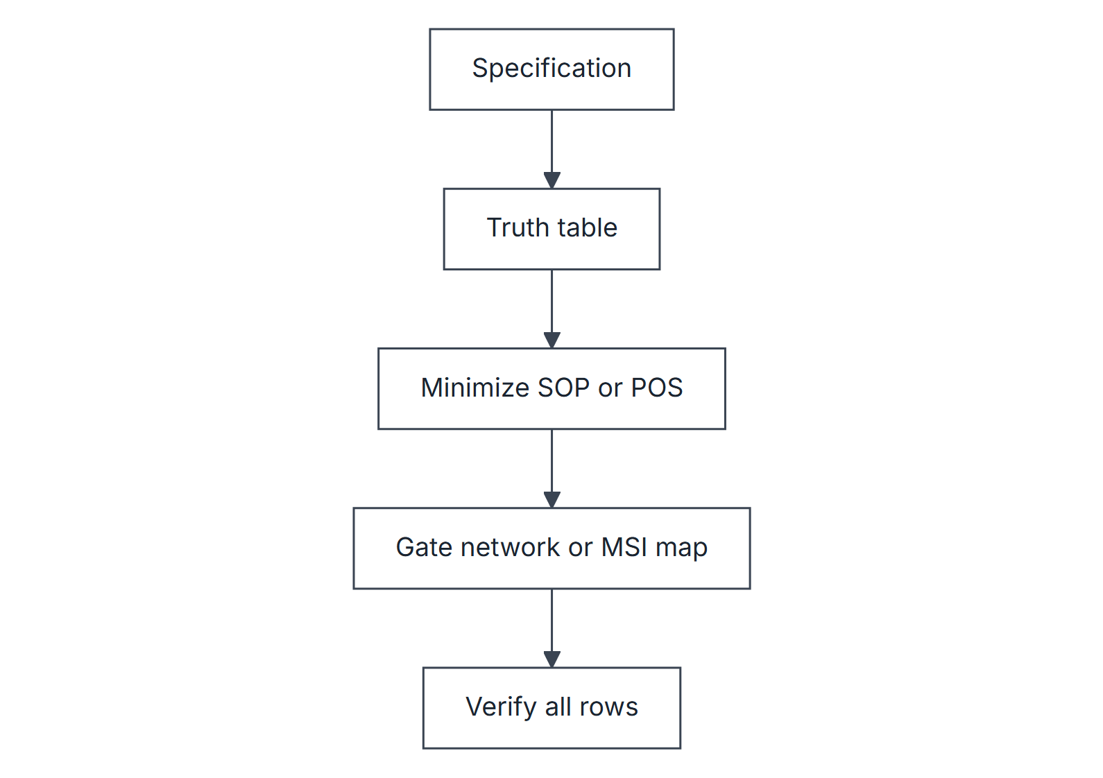
Design procedure
- State the problem: list inputs, outputs, and the meaning of each.
- Assign 0/1 encodings to symbolic values if needed.
- Build a truth table (or leave don't-cares for unused input combinations).
- Minimize each output (K-map or QM), choose SOP or POS to match available gates.
- Draw the gate diagram (or map onto MUX/decoder/ROM/PLA).
- Check the table against the circuit on every row, including don't-care decisions.
Analysis versus design
Analysis starts from a diagram and produces equations or a truth table: label every gate output, write each as a function of its inputs, and substitute from the inputs forward. Design goes the other way. Both are used in this note.
Technology mapping (exam level)
| Target | What it stores or computes | Size measure |
|---|---|---|
| Two-level gates | minimized SOP (AND-OR, NAND-NAND) or POS (OR-AND, NOR-NOR) | gates, literals |
| Multiplexer | Shannon expansion on the select inputs | one -to-1 MUX per output |
| Decoder plus OR | one OR per output over the decoder lines of its minterms | one -to- decoder |
| ROM | the whole truth table: words of bits | bits |
| PLA | programmable AND array and programmable OR array | inputs, shared products, outputs |
| PAL | programmable AND array, fixed OR array | products per output are fixed |
A ROM is a decoder (fixed AND array generating all minterms) followed by a programmable OR array, so its size does not depend on how simple the functions are. A PLA pays only for the distinct product terms the minimized outputs use, so multi-output sharing matters.
How it works
Analysis of a NAND network
Gates: , , , . Substituting and applying De Morgan once, : the majority function. A two-level NAND-NAND network is always the SOP obtained by reading every NAND as an AND in the first level and as an OR in the second.
Magnitude comparator
For -bit unsigned and , let (, bit equal). For :
The pattern extends to bits: when, at the most significant position where they differ, and . So . Exactly one of , , is 1 on every row, so any one of them can be derived from the other two: .
Parity generator and checker
An even-parity generator for data bits outputs , so that the transmitted bits contain an even number of 1s. The checker recomputes ; signals an error.
- For data , and the transmitted word has four 1s.
- A single flipped bit makes . Two flipped bits leave : parity detects every odd number of bit errors and no even number.
- data bits need two-input XOR gates in the generator; as a balanced tree the delay is XOR levels (2 levels for 4 bits, 3 for 8).
Odd parity uses instead of .
Code converter: BCD to Excess-3
Inputs (a BCD digit, the MSB), outputs equal to the digit plus 3. The six codes 1010 to 1111 never occur, so they are don't-cares. Minimizing each output with them:
Note and . If every output is forced to 0 on invalid inputs, the example becomes (9 literals instead of 5).
Binary to Gray converter
and : XOR gates in one level, delay 1. The Gray-to-binary converter is a chain, so its delay is XOR levels (see the Binary Codes note).
Algorithms and pseudocode
Pseudocode uses <- for assignment; a circuit is a directed acyclic graph of gates.
COMB-DESIGN(spec)
1  (inputs, outputs, rules) <- parse spec
2  table <- empty
3  for each input assignment x
4      if x is impossible then mark outputs don't-care
5      else set outputs from rules
6  for each output z
7      expr[z] <- minimize(column z of table)
8  circuit <- synthesize(expr)
9  assert EVAL(circuit) agrees with table on all care rows
10 return circuit

CRITICAL-PATH(circuit)              // gates in topological order
1  for each primary input v: arrival[v] <- 0
2  for each gate g in topological order
3      arrival[g] <- t_g + max over inputs u of g of arrival[u]
4  return max over outputs o of arrival[o]
COMB-DESIGN takes rows to fill the table, plus the minimization cost. CRITICAL-PATH is a longest-path computation on a DAG: time for gates and wires.
Mathematical explanation
Counting circuits by behaviour. An -input, -output combinational circuit computes a map . There are such maps, and a ROM with address bits and -bit words can hold any one of them, which is why its size is bits regardless of the function.
ROM sizing. A 4-bit by 4-bit unsigned multiplier has 8 inputs and an 8-bit product (the largest product is ), so a ROM realization needs bits. A 4-bit adder with carry-in has 9 inputs and 5 outputs: bits.
Why parity misses even errors. Flipping bit toggles because is the XOR of all received bits. Flipping bits toggles times, so ends at .
Worked examples
Example 1: majority of three
when at least two inputs are 1. Minterms . K-map: . Three 2-input ANDs and one 3-input OR; delay 2 levels.
Example 2: analysis of a product of sums
Given . Expanding, , since is the consensus of and . The minterms are . It is not the majority function: at the majority is 1 but .
Example 3: don't-care driven shrink
A three-input function is 1 on and don't-care on . As in Karnaugh Maps, the don't-cares give (2 literals) instead of (4 literals).
Example 4: critical path with unequal gate delays
Network: (AND, 2 ns), (OR, 2 ns), (NOT, 1 ns), (XOR, 3 ns). Arrival times: at 2, at 4, at 5, at 8 ns. The critical path is (or ) through all four gates, 8 ns; the path from is only 3 ns. In the unit-delay model the depth is 4.
Example 5: comparator values
For and : , , so ; ; . For : , , . Over all 16 input rows the three outputs are 1 on 4, 6 and 6 rows respectively.
Example 6: PLA sharing
Outputs and . A PLA needs only the three distinct products , , (the product is shared), while two separate two-level circuits would build four AND gates.
Important properties and observations
- Feedback with delay can create latches unintentionally; keep combinational diagrams acyclic.
- Related material. Static-1 hazards: a single input change can momentarily drop an SOP output that should stay 1 when the two adjacent 1-cells lie in different product terms. For with , a change of can glitch; adding the redundant consensus term removes the hazard (see Karnaugh Maps).
- Multi-output sharing: extract common product terms once; it matters for PLAs, not for ROMs.
- Gate count and delay trade off: a balanced tree and a chain of two-input gates have the same gate count but delays and .
Common misconceptions.
- "Combinational circuits can use flip-flops for pipelining and stay combinational." Pipelining inserts state; the block between registers is combinational, the system is sequential.
- "Don't-cares mean the output is 0." They mean the designer may choose.
- "Circuit delay is the number of gates." It is the longest path, which can be much shorter than the gate count.
- "A ROM for a simple function is smaller." ROM size is for every function of inputs and outputs.
- "Parity detects all double errors." It detects none of them.
GATE examination perspective
- TRUTH TABLE FIRST. Half the marks are encoding the word problem correctly.
- MINIMIZE EACH OUTPUT. Shared terms are a bonus when options show them.
- MSI IMPLEMENTATION. "Realize using 8:1 MUX" means Shannon expand on three select bits.
- ANALYSIS. Read a gate figure into an equation; simplify; match options.
- CRITICAL PATH. Add delays along every path and take the maximum; with unequal gate delays the deepest path need not be the slowest.
- ROM SIZE. bits; count the output width carefully (an unsigned product of two -bit numbers fits in bits, required in the worst case for ; for , one bit suffices).
- PARITY. Generator XORs; detects odd numbers of errors only.
Summary
Sources
- M. Morris Mano, M. D. Ciletti, Digital Design, 5th ed., Pearson, 2013: Chapter 3, Section 3.8 (exclusive-OR function, parity generation and checking); Chapter 4, Sections 4.2 to 4.4 (combinational circuits, analysis, design procedure) and 4.8 (magnitude comparator).