
Introduction
Memory interfacing is the design of the connection between a processor and its main memory: how memory chips of a given size are combined into a memory of the required size and word width, how each address selects exactly one location, and how the memory is organised so that it can deliver words fast enough. The processor sees one linear array of addressable locations; underneath, that array is built from many identical chips, selected by decoders driven by the high-order address bits.
GATE asks for the number of chips and decoders needed, the address lines of each chip, the address range a chip answers, the effect of incomplete decoding, the byte order of a stored word, DRAM refresh overhead, and the speed-up that memory interleaving gives. The time cost of memory inside the hierarchy is the subject of Memory Hierarchy and Performance.
Prerequisites
- Multiplexers, Decoders and Encoders: an -to- decoder activates exactly one output for each input combination; that output drives a chip-select line.
Core concepts
Memory chips
A chip described as stores words of bits. It has:
| Signal | Count | Purpose |
|---|---|---|
| Address lines | Select one of the words | |
| Data lines | Carry the word in or out | |
| Chip select (or CE) | 1 | The chip responds only when selected |
| Read/write | 1 | Direction of the transfer |
| Technology | Cell | Properties |
|---|---|---|
| SRAM | Flip-flop (about 6 transistors) | Fast, no refresh, low density; used for caches |
| DRAM | One transistor and a capacitor | Dense and cheap, slower, the charge leaks so every row must be refreshed periodically; used for main memory |
| ROM, PROM, EPROM, EEPROM, flash | Fixed or electrically programmed | Non-volatile; holds firmware and boot code |
DRAM addressing. A DRAM chip stores its cells in a square-ish array of rows and columns. To save pins, the row address and the column address share the same pins and are latched one after the other by the row-address strobe (RAS) and the column-address strobe (CAS). A chip with addressable locations then needs only address pins.
Building a memory from chips
To build an memory from chips:
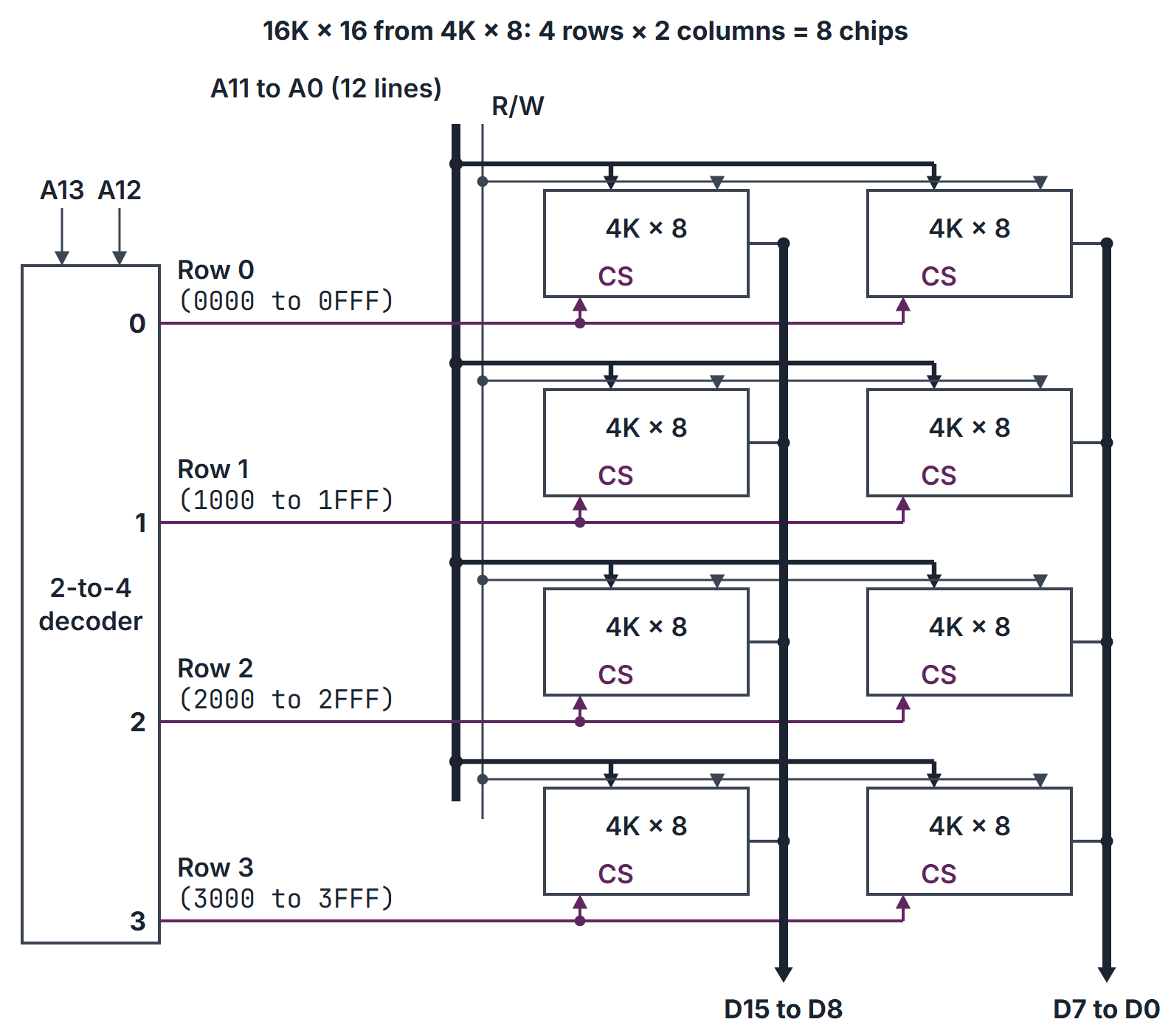
- Width expansion (more bits per word): place chips side by side. They share every address line and the chip select; each supplies of the data bits.
- Depth expansion (more words): stack rows of chips. The low address bits go to every chip; the high bits drive a decoder whose outputs select one row.
- Number of chips . Decoder: -to-.
Address decoding
- Full decoding: every address bit above the chip's own address lines takes part in selecting the chip, so each memory word has exactly one address.
- Partial (incomplete) decoding: some high-order bits are ignored. The chip then answers at different addresses, where is the number of ignored bits (aliases, foldback or mirror images). Cheaper decoders, wasted address space.
Byte order and alignment
In a byte-addressable memory, a multi-byte word occupies consecutive addresses.
- Big-endian: the most significant byte is at the lowest address.
- Little-endian: the least significant byte is at the lowest address.
- Alignment: a -byte item is aligned if its address is a multiple of . Misaligned accesses may need two memory accesses or may be forbidden.
Interleaving
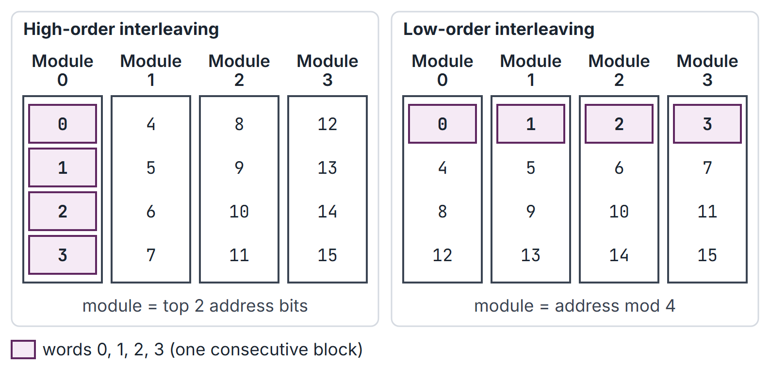
Main memory is often split into independent modules (banks), each with its own address and data registers, so that several accesses can be in progress at once.
| Scheme | Module of address | Address within module | Good for |
|---|---|---|---|
| High-order interleaving | the top bits of | the remaining bits | Expanding memory module by module; a sequential block within one module has no bank overlap; independent requests to different modules can overlap |
| Low-order interleaving | (the low bits) | Block transfers: consecutive words are in different modules, so their accesses overlap |
With low-order interleaving, a block of consecutive words keeps all modules busy at once, which is why it cuts the cache miss penalty.
How it works
Algorithms and pseudocode
DESIGN-MEMORY(M, W, N, w)                  // target M x W, chips N x w
  rows   <- M / N                          // depth expansion
  cols   <- W / w                          // width expansion
  chips  <- rows * cols
  chipAddressBits <- lg N                  // A(lgN - 1) .. A0 to every chip
  decoderInputs   <- lg rows               // next address bits
  return (chips, rows, cols, decoderInputs)

SELECT(address)                            // full decoding
  row    <- floor(address / N)             // decoder output that goes active
  within <- address mod N                  // word inside every chip of that row
  return (row, within)
Every quantity is a power of 2 in practice, so the divisions are bit-field splits of the address.
Mathematical explanation
Address bits. A memory of addressable units needs address bits. A chip of words uses of them; the decoder uses ; the two add up to .
Chip address range (full decoding). Row answers addresses to .
Aliases (partial decoding). If address bits are unused, each location appears at addresses.
DRAM refresh overhead. If a chip has rows, each row refresh takes , and every row must be refreshed once per period , then the fraction of time unavailable for normal accesses is .
Interleaved block read. With low-order-interleaved modules, memory access latency before the bus transfer, with each bank remaining occupied until its subsequent transfer ends, and a bus that moves one word per , a block of consecutive words takes about instead of .
Worked examples
Example 1: chips and decoder (Figure 1)
Build a memory ( words) from chips.
- Chips: .
- Address bits: 14 in total. A11 to A0 (12 bits) go to every chip; A13 and A12 drive a 2-to-4 decoder.
- Address ranges (hexadecimal, word addresses): row 0
0000to0FFF, row 11000to1FFF, row 22000to2FFF, row 33000to3FFF. - Address
2ABC: A13 A12 , so row 2 is selected, wordABCinside both chips of that row.
Example 2: partial decoding
A chip sits in a 16-bit address space. Its select logic checks only A15 and A14 ; A13 to A10 are ignored and A9 to A0 go to the chip. The chip responds to every address from 8000 to BFFF: aliases of each byte, for example 8000, 8400, 8800, ..., BC00 all reach byte 0. Adding A13 to A10 to the select logic (all four 0) would confine the chip to 8000 to 83FF.
Example 3: interleaving speed
Each module needs 80 ns per access, and the bus moves one word in 20 ns; a module stays busy until its word has been transferred. Read 8 consecutive words.
- One module, or high-order interleaving when the 8 words lie inside the same module: ns.
- Four low-order-interleaved modules: words 0 to 3 are ready at 80 ns and leave at 100, 120, 140 and 160 ns; modules 0 to 3 then start words 4 to 7 at 100, 120, 140 and 160 ns, which leave at 200, 220, 240 and 260 ns. Total 260 ns, a speed-up of about 3.1.
Example 4: DRAM refresh
A DRAM has rows, each row must be refreshed every 64 ms, and one row refresh takes 50 ns. Refresh time per period: ns s, so ms of the time is spent refreshing. Spreading the refreshes evenly means one row every s.
Example 5: byte order
The 32-bit value 0x12345678 is stored at byte address 100.
| Address | 100 | 101 | 102 | 103 |
|---|---|---|---|---|
| Big-endian | 12 | 34 | 56 | 78 |
| Little-endian | 78 | 56 | 34 | 12 |
Reading the byte at address 100 gives 0x12 on a big-endian machine and 0x78 on a little-endian one; reading the 16-bit half-word at 100 gives 0x1234 and 0x5678.
Example 6: DRAM pins
A DRAM has locations, so 18 address bits. With row and column addresses multiplexed on the same pins (9 row bits, then 9 column bits), it needs only 9 address pins and 4 data pins.
Important properties and observations
- Chips in one row share the address and select lines; chips in one column share the data lines.
- The decoder uses the high-order bits in depth expansion; the low-order bits go to every chip.
- Partial decoding saves logic but creates aliases; two devices whose aliases overlap would conflict.
- Low-order interleaving helps sequential access; high-order interleaving can overlap independent requests to different modules, from one or more request sources, but not a sequential block wholly inside one module.
- Endianness matters only for multi-byte items. A byte array looks the same on both.
- DRAM refresh overhead is small but must be included when a question asks for the available bandwidth.
- Common misconceptions.
- "Number of chips ." Width expansion multiplies it by .
- "A 4K chip needs 4 address lines." It needs .
- "Interleaving makes one access faster." Each access still takes the module's full access time; interleaving overlaps accesses.
GATE examination perspective
- CHIP COUNT. , after converting both to the same units.
- DECODER SIZE. -to-rows; for width expansion only, no decoder is needed.
- ADDRESS RANGE. Fix the decoder bits for the chosen row; the chip bits run from all 0s to all 1s.
- ALIASES. Count the address bits that neither the chip nor the decoder uses: copies.
- INTERLEAVED TIMING. Draw the module timeline; low-order interleaving overlaps consecutive requests; high-order interleaving can overlap independent requests to different modules.
- REFRESH. Rows times refresh time divided by the refresh period.
- BYTE ORDER. Write the bytes out address by address before answering.
Summary
Sources
- C. Hamacher, Z. Vranesic, S. Zaky, Computer Organization, 5th ed., McGraw-Hill, 2002, Chapter 2, Section 2.2 (Memory Locations and Addresses, including 2.2.2 Big-endian and Little-endian Assignments and 2.2.3 Word Alignment); Chapter 5, Sections 5.2 (Semiconductor RAM Memories, including 5.2.1 Internal Organization of Memory Chips and 5.2.5 Structure of Larger Memories), 5.3 (Read-Only Memories) and 5.6.1 (Interleaving).
- W. Stallings, Computer Organization and Architecture, 10th ed., Pearson: Section 5.1 (Semiconductor Main Memory).